| CPC H10K 50/17 (2023.02) [H10K 50/11 (2023.02); H10K 59/35 (2023.02); H10K 85/115 (2023.02); H10K 85/141 (2023.02); H10K 85/146 (2023.02); H10K 50/115 (2023.02); H10K 50/16 (2023.02); H10K 59/12 (2023.02); H10K 2101/40 (2023.02); H10K 2102/00 (2023.02); H10K 2102/331 (2023.02); H10K 2102/351 (2023.02)] | 25 Claims |

|
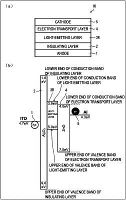
1. A light-emitting element provided with
an anode,
a light-emitting layer including quantum dots, and
a cathode,
the light-emitting element comprising:
an electron transport layer provided between the cathode and the light-emitting layer; and
a hole tunneling insulating layer provided between the anode and the light-emitting layer and in contact with the anode and the light-emitting layer, wherein
the hole tunneling insulating layer includes a plurality of layers composed of different materials.
|