| CPC H10B 43/50 (2023.02) [H01L 21/76805 (2013.01); H01L 21/76895 (2013.01); H01L 23/535 (2013.01); H10B 41/27 (2023.02); H10B 41/41 (2023.02); H10B 41/50 (2023.02); H10B 43/27 (2023.02); H10B 43/40 (2023.02)] | 18 Claims |

|
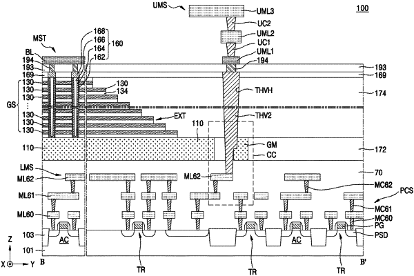
1. An integrated circuit device comprising:
a substrate;
a peripheral circuit structure disposed on the substrate, wherein the peripheral circuit structure includes a peripheral circuit and a lower wiring connected to the peripheral circuit;
a conductive plate covering a portion of the peripheral circuit structure;
a cell array structure disposed on the peripheral circuit structure with the conductive plate therebetween, wherein the cell array structure includes a memory cell array and an insulation layer surrounding the memory cell array;
a through hole via passing through the insulation layer, wherein the through hole via connects to the lower wiring and extends in a direction vertical to a top surface of the substrate; and
an etch guide member disposed outside of the conductive plate in the insulation layer at the same level as the conductive plate, wherein:
wherein the conductive plate is configured to transfer a common source voltage to the memory cell array,
the through hole via is disposed between the etch guide member and the conductive plate and contacts the etch guide member on a first side of the through hole via, and
wherein the through hole via contacts the insulation layer on a second side of the through hole via opposite to the first side.
|