| CPC H10B 43/27 (2023.02) [H01L 23/5226 (2013.01); H01L 23/53271 (2013.01); H01L 23/53295 (2013.01); H01L 29/0847 (2013.01); H01L 29/40117 (2019.08)] | 14 Claims |
|
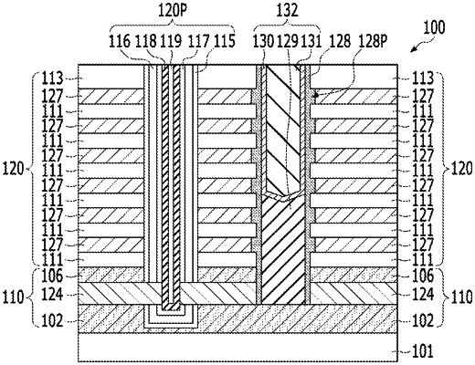
1. A method for fabricating a semiconductor device, comprising:
forming a first multi-layer stack including liner layers and a source sacrificial layer over a lower structure;
forming a second multi-layer stack including dielectric layers and sacrificial layers over the first multi-layer stack;
forming a vertical contact recess extending through the second multi-layer stack and the source sacrificial layer;
replacing the source sacrificial layer with a source contact layer;
replacing the sacrificial layers with conductive layers;
forming a seed layer on a sidewall of the vertical contact recess to seal the conductive layers;
forming a carbon-containing spacer on the seed layer; and
forming a source contact plug in the vertical contact recess.
|