| CPC H10B 43/27 (2023.02) [H01L 21/31111 (2013.01); H01L 21/32134 (2013.01); H01L 29/40114 (2019.08); H01L 29/40117 (2019.08); H10B 41/27 (2023.02); H10B 41/35 (2023.02); H10B 43/35 (2023.02); H10B 99/00 (2023.02)] | 11 Claims |

|
1. A method of forming vertically-stacked memory cells, comprising:
forming an opening through a stack of alternating insulative and conductive levels, the forming the opening producing insulative sidewalls along the insulative levels and conductive material sidewalls along the conductive levels;
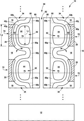
after the forming the opening, forming recessed conductive material sidewalls along the conductive levels by removing conductive material of the conductive levels to form cavities extending into the conductive levels, the recessed conductive material sidewalls being concave surfaces extending along the conductive levels, with upper and lower portions of the insulative levels being exposed within the cavities, regions of the insulative levels remaining as ledges extending from the recessed conductive material sidewalls to the insulative sidewalls;
after the removing the conductive material, removing material from the ledges to thin the ledges into thinned ledges extending from the recessed conductive material sidewalls, an entirety of the thinned ledges being curved; and
after the removing the material from the ledges, forming charge-blocking dielectric and charge-storage structures within the cavities.
|