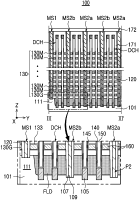
| CPC H10B 41/27 (2023.02) [H10B 41/10 (2023.02); H10B 43/10 (2023.02); H10B 43/27 (2023.02)] | 20 Claims |

|
1. A method for manufacturing a semiconductor device, the method comprising:
preparing a substrate comprising a first region and a second region;
forming insulating patterns in the second region and defining an active structure of the substrate;
forming a preliminary stacked structure on the substrate by alternately stacking sacrificial layers and interlayer insulating layers;
forming a channel structure penetrating through the preliminary stacked structure in the first region;
forming openings penetrating through the preliminary stacked structure and each having a trench shape extending in a first direction;
removing the sacrificial layers through the openings;
forming gate electrodes by forming a first conductive material in regions from which the sacrificial layers were removed;
forming a separation insulating layer covering sidewalls of the openings; and
forming separation regions by forming a second conductive material in the openings,
wherein the openings comprise:
first openings spaced apart from each other in a second direction that is perpendicular to the first direction and exposing the active structure;
second main openings between the first openings, spaced apart from each other in the first direction, and penetrating through respective portions of the insulating patterns; and
second auxiliary openings in the second region, spaced apart from the first openings and the second main openings in the second direction, spaced apart from each other in the first direction, and penetrating through respective portions of the insulating patterns.
|