| CPC H10B 12/31 (2023.02) [G11C 5/063 (2013.01); H01L 23/5226 (2013.01); H01L 23/5283 (2013.01); H01L 27/0688 (2013.01); H01L 29/78696 (2013.01); H10B 12/30 (2023.02)] | 20 Claims |

|
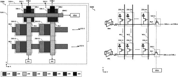
1. An integrated circuit (IC) device, comprising:
an arrangement that includes two or more memory cells, a transistor, and a bitline; and
an interconnect structure,
wherein:
an individual memory cell of the arrangement includes an access transistor,
each of the transistor and the access transistor includes a first region and a second region, wherein one of the first region and the second region is a source region and another one of the first region and the second region is a drain region,
the first regions of the access transistors of the two or more memory cells of the arrangement are directly electrically connected to one another and to the bitline, and the bitline is directly electrically connected to the first region of the transistor, and
the second region of the transistor is directly electrically connected to the interconnect structure.
|