| CPC H05K 5/0069 (2013.01) [H01R 12/71 (2013.01); H05K 5/0065 (2013.01); H05K 5/0247 (2013.01)] | 16 Claims |

|
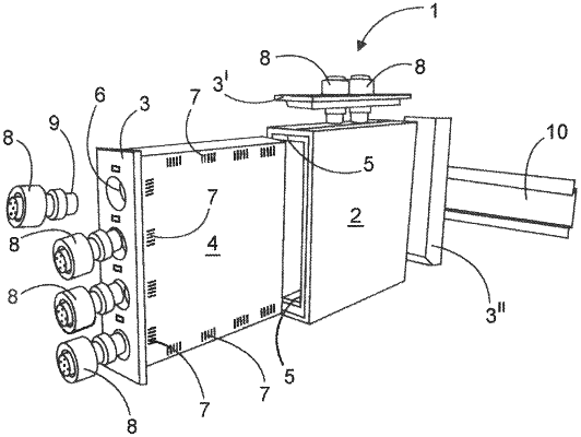
1. A system comprising: a housing, a printed circuit board arranged in the housing and a plurality of functional elements, wherein
the housing has at least one changeable side
having openings which correlate to electrical connections of the printed circuit board,
wherein the functional elements are configured to extend through the openings in the at least one changeable side and connect to the associated electrical connections of the printed circuit board, wherein each of the functional elements have on a connection side, an axial slot which extends over or around an associated connection of the printed circuit board, wherein a width of the axial slot is smaller than a thickness of the circuit board, and
wherein the printed circuit board has a rectangular basic form, wherein the electrical connections for the functional elements are arranged at edges of the printed circuit board, and wherein the electrical connections each comprise a plurality of contact plates, which are each connected to at least one trace of the printed circuit board in an electrically conductive manner.
|