| CPC H05K 3/4084 (2013.01) [H05K 1/0298 (2013.01); H05K 1/05 (2013.01); H05K 1/116 (2013.01); H05K 3/445 (2013.01); H05K 3/4647 (2013.01); H05K 2203/0323 (2013.01); H05K 2203/1484 (2013.01)] | 6 Claims |
|
1. A manufacturing method for a double-sided wiring circuit board, the method comprising:
a first step of preparing a laminate including:
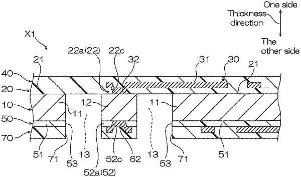
a metal core layer,
a first insulating layer disposed at one side in a thickness direction of the metal core layer, and having a first region and at least one first opening adjacent to the first region, the first region having a first hole,
a first conductor layer having a first wiring portion and a first conductive portion, the first wiring portion being disposed at least on the first region at one side in the thickness direction of the first insulating layer, the first conductive portion being disposed in the first hole and connected to the first wiring portion and the metal core layer,
a second insulating layer disposed at an opposite side in the thickness direction of the metal core layer, and having a second region and at least one second opening adjacent to the second region, the second region including a part facing to the first region in the thickness direction, the second region having a second hole in the part, and
a second conductor layer having a second wiring portion and a second conductive portion, the second wiring portion being disposed at least on the second region at an opposite side in the thickness direction of the second insulating layer, the second conductive portion being disposed in the second hole and connected to the second wiring portion and the metal core layer; and
a second step of forming a via portion in the metal core layer by a first etching treatment on the metal core layer through the first opening from one side in the thickness direction of the laminate, and by a second etching treatment on the metal core layer through the second opening from an opposite side in the thickness direction of the laminate, the via portion being surrounded by a space, extending between the first region and the second region in the thickness direction, and being connected to the first conductive portion and the second conductive portion.
|