| CPC H05K 3/3494 (2013.01) [B23K 1/0016 (2013.01); B23K 37/04 (2013.01); H05K 3/341 (2013.01); H05K 3/3457 (2013.01); B23K 2101/42 (2018.08)] | 16 Claims |

|
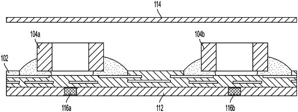
1. A method of soldering one or more components to a substrate, the method comprising:
providing a substrate having a top planar surface and a bottom planar surface;
applying an amount of solder material to at least a portion of the top planar surface of the substrate;
mounting one or more electrical components on the solder material, each of the one or more electrical components having a position and orientation relative to the substrate;
providing a carrier having a top carrier surface and a bottom carrier surface, and one or more magnets disposed between the top and bottom carrier surfaces;
positioning the substrate above the carrier such that the bottom planar surface of the substrate is above the top carrier surface and each of the one or more magnets is positioned directly below a corresponding electrical component of the one or more electrical components;
positioning a carrier cover above the top planar surface of the substrate such that there is a gap between the carrier cover and the one or more electrical components; and
heating the solder material to a predetermined temperature for a predetermined amount of time to cause the solder material to melt; and
during heating of the solder material, exerting, by each of the one or more magnets, a magnetic force on a corresponding electrical component of the one or more electrical components to maintain the orientation of the corresponding electrical component relative to the substrate while the solder material melts.
|