| CPC H05K 1/183 (2013.01) [H05K 1/113 (2013.01); H05K 2201/0166 (2013.01); H05K 2201/09036 (2013.01)] | 20 Claims |
|
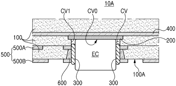
1. An electronic component embedded substrate comprising:
an insulating material including a cavity disposed in one surface thereof;
a protective layer embedded in the insulating material and covering an entire bottom surface of the cavity;
solders disposed on side surfaces of the cavity; and
an electronic component disposed in the cavity and at least partially in contact with the solders,
wherein the protective layer has a material different from that of the insulating material, and
wherein the protective layer includes an insulative material.
|