| CPC H05K 1/115 (2013.01) [H05K 3/067 (2013.01); H05K 3/423 (2013.01); H05K 2201/09227 (2013.01); H05K 2201/09563 (2013.01)] | 16 Claims |

|
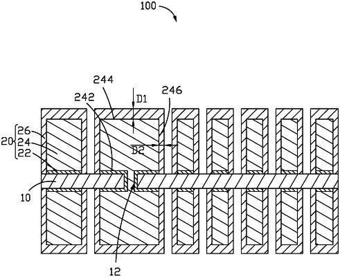
1. A circuit board, comprising:
a substrate; and
a plurality of traces spaced apart from each other on the substrate, wherein each of the plurality of traces comprises:
a seed layer on a surface of the substrate;
a first copper layer on a surface of the seed layer away from the substrate; and
a second copper layer formed on the surface of the substrate by electroplating, and the second copper layer enclosing the seed layer and the first copper layer;
wherein a ratio of a thickness of each of the plurality of traces to a pitch between any two adjacent ones of the plurality of traces is greater than 1; the first copper layer comprises a lower surface in direct contact with the seed layer, an upper surface opposite to the lower surface, and a side surface connecting the lower surface and the upper surface;
a thickness of the second copper layer covering the upper surface of the first copper layer is defined as a first thickness, and a thickness of the second copper layer covering the side surface of the first copper layer is defined as a second thickness; and
the first thickness is greater than the second thickness;
wherein the first thickness is at least twice as thick as the second thickness.
|