| CPC H05K 1/0218 (2013.01) [H05K 1/115 (2013.01); H05K 3/42 (2013.01); H05K 2201/09518 (2013.01); H05K 2201/09545 (2013.01)] | 14 Claims |

|
1. An information handling system comprising:
a printed circuit board;
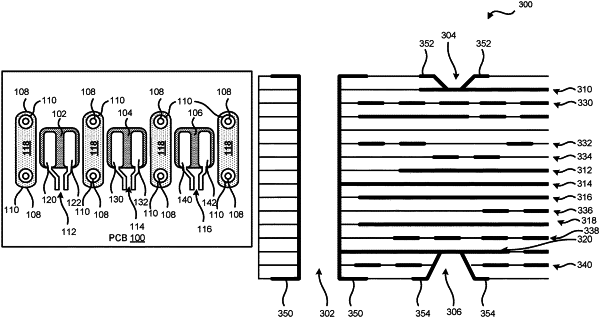
a surface mount connector mounted on the printed circuit board, the surface mount connector includes first and second surface mount connector portions;
a first differential pair on the first surface mount connector portion;
a second differential pair on the second surface mount connector portion;
a ground pad of the surface mount connector located in between the first and second surface mount connector portions;
a first ground via in physical communication with a first ground plane within the printed circuit board, with the ground pad of the surface mount connector, and with a first ground pad on a surface of the printed circuit board, wherein the first ground via is a micro-via, wherein the first ground pad is in physical communication with the ground pad of the surface mount connector; and
a second ground via in physical communication with a second ground plane within the printed circuit board, with the ground pad of the surface mount connector, and with a second ground pad on the surface of the printed circuit board, wherein a signal layer is located in a plane of the printed circuit board in between a surface of the printed circuit board and the second ground plane, wherein the second ground pad is in physical communication with the ground pad of the surface mount connector, wherein the second ground via is a skip via, wherein the first and second ground pads are on a same surface of the printed circuit board, wherein the first and second ground vias extend from the surface of the printed circuit board to respective ones of the first and second ground planes within the printed circuit board.
|