| CPC H05K 1/0209 (2013.01) [H05K 1/09 (2013.01); H05K 2201/0355 (2013.01)] | 5 Claims |

|
1. A circuit board comprising:
an insulating substrate; and
a circuit pattern of a metal formed on the insulating substrate in direct contact with the insulating substrate,
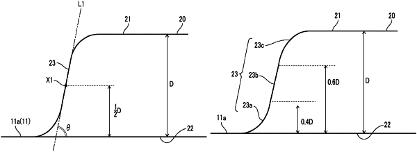
wherein a side surface of the circuit pattern has a region in which an angle formed by a surface of the insulating substrate and a tangential line at a middle portion in a height direction in a cross-sectional view perpendicular to an extending direction of the metal is 80 degrees or more and 100 degrees or less,
wherein in a case where a height of the circuit pattern is denoted by D, the side surface of the circuit pattern exhibits a straight line in the cross-sectional view perpendicular to the extending direction of the metal, in a height range of 0.4D or more and 0.6D or less in a perpendicular direction from the insulating substrate, and
wherein the side surface of the circuit pattern exhibits a trailing-tailed shape at an interface with the insulating substrate.
|