| CPC H05K 1/0206 (2013.01) [H01L 23/367 (2013.01); H01L 23/38 (2013.01); H05K 1/0298 (2013.01); H05K 1/183 (2013.01); H05K 3/30 (2013.01); H01L 23/13 (2013.01); H10N 10/13 (2023.02)] | 18 Claims |

|
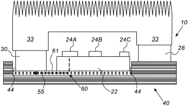
1. A semiconductor device assembly, comprising:
a multi-layer printed circuit board (PCB) comprising a lateral heat conducting path formed in a recessed area of the PCB;
a thermoelectric cooler (TEC) and a chip disposed on the PCB, side-by-side to one another within the recessed area, such that entire bottom surfaces of both the chip and the TEC are mounted directly on the lateral heat conducting path, wherein the TEC is configured to evacuate heat from the chip via the lateral heat conducting path, and to dissipate the evacuated heat via a first end of a heat sink in thermal contact with the TEC; and
packaged integrated circuitry (IC) disposed on an un-recessed area of the PCB, wherein the packaged IC is configured to dissipate heat via a second end of the heat sink that is in thermal contact with the packaged IC.
|