US 12,114,088 B2
Solid-state imaging device and method of operating the same, and electronic apparatus and method of operating the same
Takeshi Takeda, Kanagawa (JP)
Assigned to Sony Semiconductor Solutions Corporation, Kanagawa (JP)
Filed by Sony Semiconductor Solutions Corporation, Kanagawa (JP)
Filed on Mar. 21, 2023, as Appl. No. 18/187,274.
Application 18/187,274 is a continuation of application No. 17/371,928, filed on Jul. 9, 2021, granted, now 11,627,275.
Application 17/371,928 is a continuation of application No. 16/722,629, filed on Dec. 20, 2019, granted, now 11,070,760, issued on Jul. 20, 2021.
Application 16/722,629 is a continuation of application No. 16/132,903, filed on Sep. 17, 2018, granted, now 10,574,924, issued on Feb. 25, 2020.
Application 16/132,903 is a continuation of application No. 15/814,741, filed on Nov. 16, 2017, granted, now 10,104,327, issued on Oct. 16, 2018.
Application 15/814,741 is a continuation of application No. 15/397,252, filed on Jan. 3, 2017, granted, now 9,832,410, issued on Nov. 28, 2017.
Application 15/397,252 is a continuation of application No. 14/950,715, filed on Nov. 24, 2015, granted, now 9,571,776, issued on Feb. 14, 2017.
Application 14/950,715 is a continuation of application No. 14/492,643, filed on Sep. 22, 2014, granted, now 9,282,262, issued on Mar. 8, 2016.
Claims priority of application No. 2013-197874 (JP), filed on Sep. 25, 2013.
Prior Publication US 2023/0308782 A1, Sep. 28, 2023
This patent is subject to a terminal disclaimer.
Int. Cl. H04N 25/75 (2023.01); H04N 25/59 (2023.01); H04N 25/626 (2023.01); H04N 25/709 (2023.01); H04N 25/77 (2023.01); H04N 25/771 (2023.01)
CPC H04N 25/75 (2023.01) [H04N 25/59 (2023.01); H04N 25/626 (2023.01); H04N 25/709 (2023.01); H04N 25/77 (2023.01); H04N 25/771 (2023.01)] 14 Claims
OG exemplary drawing
 
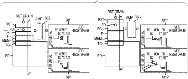
1. A light detecting device, comprising:
a photoelectric conversion region,
a first charge holding region configured to receive a charge from the photoelectric conversion region,
a first transistor electrically connected to the photoelectric conversion region and the first charge holding region, and
a second transistor including a first terminal electrically connected to the photoelectric conversion region through the first transistor, and a second terminal electrically connected to a reset drain, wherein,
in a plan view, the second transistor and the first charge holding region are disposed at a same side of the photoelectric conversion region along a first direction that extends orthogonally from the same side of the photoelectric conversion region.