| CPC H03K 3/35613 (2013.01) [G11C 7/065 (2013.01); G11C 27/02 (2013.01); H03M 1/1245 (2013.01)] | 8 Claims |

|
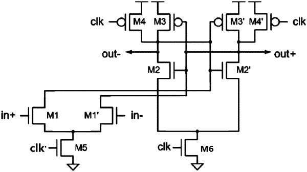
1. A high-speed sampling circuit comprising:
a sampling module configured for amplifying a differential input signal;
a latch module configured for latching a differential output signal of the sampling module;
a first control module configured for controlling the sampling module under a first clock signal;
a second control module configured for controlling the latch module under a second clock signal; and
a third control module for controlling the output of the differential output signal under the second clock signal;
wherein during a first stage from time point T0 to time point T1, both the first clock signal and the second clock signal are each 0, both the sampling module and the latch module are turned off, and both the first differential output node and the second differential output node are operative to be pulled up to a power supply voltage;
wherein during a second stage from time point T1 to time point T2, both the first clock signal and the second clock signal are each 1, both the sampling module and the latch module are turned on, and a voltage difference between the first differential input node and the second differential input node is operative to cause the latch module to enter an unbalanced state;
wherein during a third stage from time point T2 to time point T3, the first clock signal is 0, the sampling module is turned off, and the unbalanced state of two branches of the latch module is amplified through a positive feedback, so that an input state sampled in the T1 to T2 stage is output through the first differential output node and the second differential output node;
wherein during a fourth stage from time point T3 to time point T4, both the first clock signal and the second clock signal are each 0, and the high-speed sampling circuit is operative to return to the reset state in the first stage from the time point T0 to the time point T1.
|