| CPC H03K 21/02 (2013.01) [H05K 1/0296 (2013.01); H04B 1/04 (2013.01)] | 18 Claims |

|
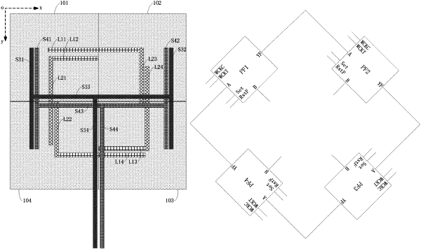
1. A layout structure, comprising:
a frequency divider pattern layer comprising a first frequency divider region, a second frequency divider region, a third frequency divider region and a fourth frequency divider region arranged centrosymmetrically; and
a conductor pattern layer formed on the frequency divider pattern layer, the conductor pattern layer comprising a first sub-conductor pattern layer and a second sub-conductor pattern layer stacked;
wherein the first sub-conductor pattern layer is configured to communicate the first frequency divider region with the second frequency divider region, and communicate the third frequency divider region with the fourth frequency divider region; and
the second sub-conductor pattern layer is configured to communicate the first frequency divider region with the fourth frequency divider region, and communicate the second frequency divider region with the third frequency divider region;
the first frequency divider region is configured to form a first frequency divider, the second frequency divider region is configured to form a second frequency divider, the third frequency divider region is configured to form a third frequency divider, and the fourth frequency divider region is configured to form a fourth frequency divider; and
the first sub-conductor pattern layer comprises a first conductor pattern, a second conductor pattern, a third conductor pattern, and a fourth conductor pattern,
wherein the first conductor pattern communicates an output terminal of the first frequency divider with a first data input terminal of the second frequency divider;
the second conductor pattern is connected to a second data input terminal of the second frequency divider;
the third conductor pattern is connected to a second data input terminal of the fourth frequency divider; and
the fourth conductor pattern communicates an output terminal of the third frequency divider with a first data input terminal of the fourth frequency divider.
|