| CPC H03K 19/1774 (2013.01) [H03K 5/15093 (2013.01); H03K 17/28 (2013.01)] | 13 Claims |

|
1. A microelectronic circuit, comprising:
a plurality of logic units and register circuits, said plurality of logic units and register circuits arranged into a plurality of processing paths; and
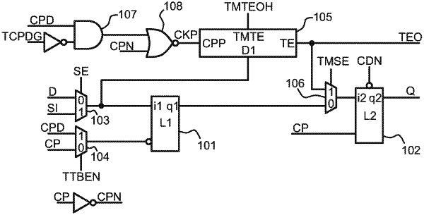
at least one monitor circuit associated with a first register circuit of said plurality of register circuits, said at least one monitor circuit being configured to produce a timing event observation signal as a response to a change in a digital value at an input of the first register circuit that took place later than an allowable time limit defined by a triggering signal to said first register circuit;
wherein a first processing path of said plurality of processing paths goes through a first logic unit of said plurality of logic units to said first register circuit,
and wherein said first processing path is a delay-critical processing path due to an amount of delay that it is likely to generate,
and wherein the microelectronic circuit comprises, on the first processing path leading to said first logic unit, a controllable data event injection point for controllably generating a change of a digital value propagating to said first logic unit irrespective of what other data is processed on said first processing path,
and wherein said microelectronic circuit is configured to freeze a first digital value stored in said first register circuit for a time during which the change generated through said controllable data event injection point propagates to said first register circuit.
|