| CPC H03K 17/161 (2013.01) | 15 Claims |

|
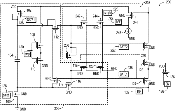
1. A bootstrap switch circuit, comprising:
a transistor-based switch controlled by a first gate signal;
a leakage protection transistor configured to be controlled by a second gate signal and connected in series with the transistor-based switch and configured to reduce gate induced drain leakage in the transistor-based switch;
a first gate driver configured to produce a first gate signal at its output, wherein the first gate signal is configured to turn on the transistor-based switch during a sampling mode in which the bootstrap switch circuit is configured to sample an input voltage and turn off the transistor-based switch during a hold mode in which the bootstrap switch circuit is configured to hold a sampled input voltage; and
a second gate driver configured to produce a second gate signal at its output and to receive an output signal of the bootstrap switch circuit, wherein the second gate signal is configured to turn on the leakage protection transistor during the sampling mode and turn off the leakage protection transistor during the hold mode and wherein the second gate signal is based upon the output signal of the bootstrap switch circuit.
|