| CPC H03H 9/25 (2013.01) [H03H 9/02559 (2013.01); H03H 9/02866 (2013.01); H03H 9/14541 (2013.01)] | 18 Claims |

|
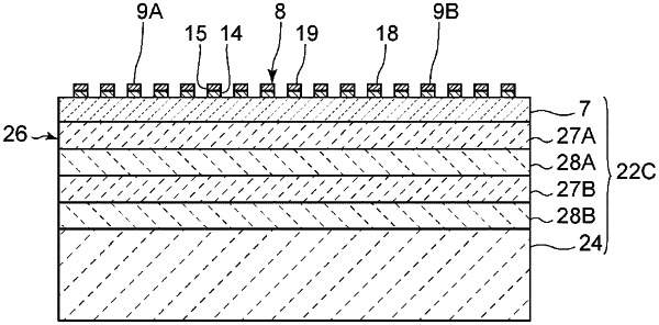
1. An acoustic wave device comprising:
an energy confinement layer;
a piezoelectric layer on the energy confinement layer and made of Y-cut X-propagation lithium tantalate having a cut angle of equal to or more than about −10° and equal to or less than about 65°; and
an IDT electrode on the piezoelectric layer; wherein
the IDT electrode includes a plurality of electrode fingers, the plurality of electrode fingers including a multilayer body including an Al metal layer defined by an Al layer or an alloy layer including Al, and a high acoustic impedance metal layer that has a Young's modulus equal to or more than about 200 GPa and a higher acoustic impedance than an acoustic impedance of Al;
the high acoustic impedance metal layer is closer to the piezoelectric layer than the Al metal layer;
when a wavelength defined by an electrode finger pitch of the IDT electrode is denoted by λ and a wavelength specific film thickness of the piezoelectric layer is denoted by tLT, tLT≤1λ is satisfied; and
a total of normalized film thicknesses obtained by normalizing a film thickness of each layer of the plurality of electrode fingers by a density and a Young's modulus of the Al metal layer is denoted by T, the expression T≤0.1125tLT+0.0574 is satisfied.
|