| CPC H03H 11/24 (2013.01) [H04B 1/1607 (2013.01); H04W 88/08 (2013.01)] | 24 Claims |

|
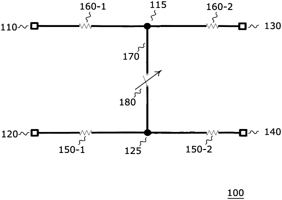
1. An attenuator circuit, comprising:
a first input node and a second input node each configured to receive a respective one of a first input signal and a second input signal forming a differential input signal pair;
a first plurality of resistive elements coupled in series between the first input node and a first output node for outputting a first output signal;
a second plurality of resistive elements coupled in series between the second input node and a second output node for outputting a second output signal;
a first shunt path coupled to a first intermediate node and a second intermediate node, the first intermediate node being arranged between two resistive elements of the first plurality of resistive elements, the second intermediate node being arranged between two resistive elements of the second plurality of resistive elements, wherein the first shunt path comprises a first switch circuit configured to selectively couple the first intermediate node and the second intermediate node based on one or more first control signals; and
a second shunt path coupled to a third intermediate node and a fourth intermediate node, the third intermediate node being arranged between two resistive elements of the first plurality of resistive elements, the fourth intermediate node being arranged between two resistive elements of the second plurality of resistive elements, and wherein the second shunt path comprises a second switch circuit configured to selectively couple the third intermediate node and the fourth intermediate node based on one or more second control signals.
|