| CPC H03H 11/0461 (2013.01) [H03M 1/0626 (2013.01); H03M 1/66 (2013.01); H04B 1/04 (2013.01)] | 24 Claims |

|
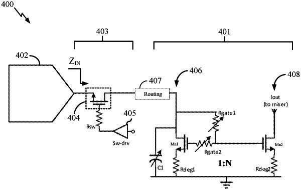
1. A filter circuit comprising:
an input node;
an output node;
a power supply node;
a first transistor comprising a drain coupled to the input node;
a second transistor comprising a drain coupled to the output node and comprising a gate coupled to a gate of the first transistor;
a capacitive element coupled between the drain of the first transistor and the power supply node;
a first resistive element coupled between the drain and the gate of the first transistor;
a first source degeneration element coupled between a source of the first transistor and the power supply node;
a second source degeneration element coupled between a source of the second transistor and the power supply node;
a switch coupled between the input node and the drain of the first transistor;
a switch driver; and
a second resistive element coupled between a control input of the switch and an output of the switch driver.
|