| CPC H03F 1/223 (2013.01) [H03F 1/0233 (2013.01); H03F 1/26 (2013.01); H03F 3/195 (2013.01); H03F 2200/294 (2013.01); H03F 2200/451 (2013.01)] | 21 Claims |

|
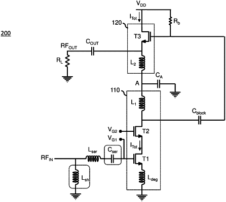
1. A stacked multi-stage low noise amplifier (LNA) circuit, comprising:
a first amplification stage comprising a common-source amplifier coupled between a common node and a reference ground, the first amplification stage configured to receive an input radio frequency (RF) signal and generate therefrom a first stage amplified RF signal;
a second amplification stage comprising a common-drain amplifier coupled between a supply voltage and the common node, the second amplification stage configured to receive the first stage amplified RF signal and generate therefrom an output RF signal to a load; and
a shunting capacitor coupled to the common node, the shunting capacitor configured to short the common node to the reference ground at frequencies of operation of the first and second amplification stages;
the common-source amplifier comprising an input transistor, the input transistor comprising:
a gate that is coupled to the input RF signal;
a source that is coupled to the reference ground through a degeneration inductor; and
a drain that is coupled to the common node through a first stage load inductor;
the common-drain amplifier comprising a source-follower transistor, the source-follower transistor comprising:
a gate that is coupled to the drain of the input transistor to receive the first stage amplified RF signal;
a drain that is coupled to the supply voltage; and
a source that is coupled to the common node through a second stage load inductor, the source also being coupled to the load.
|