| CPC H02M 7/217 (2013.01) [H02M 1/0009 (2021.05); H02M 1/08 (2013.01)] | 7 Claims |

|
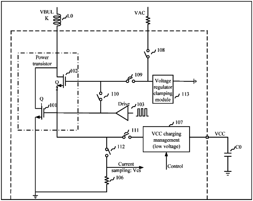
1. A power supply control circuit for a switching power supply system, comprising: a power transistor and current sampling module, a voltage common collector (VCC) charging management module, a switch module, and a voltage regulator clamping module, wherein
the power transistor and current sampling module comprises: a main switch high-voltage power transistor, a power transistor driver, an auxiliary sampling high-voltage transistor, and a current sampling resistor;
the switch module comprises a first switch, a second switch, a third switch, and a fourth switch;
the main switch high-voltage power transistor comprises a drain connected to a drain of the auxiliary sampling high-voltage transistor, a source grounded, and a gate connected to an output terminal of the power transistor driver; and the auxiliary sampling high-voltage transistor comprises a gate connected to one terminal of the first switch and one terminal of the second switch and a source connected to one terminal of the third switch and one terminal of the fourth switch; and
an other terminal of the first switch is connected to one terminal of the voltage regulator clamping module; the one terminal of the voltage regulator clamping module is further connected to an external voltage regulator clamping bias resistor, and an other terminal of the voltage regulator clamping module is grounded; an other terminal of the second switch is connected to the output terminal of the power transistor driver; an other terminal of the third switch is connected to one terminal of the VCC charging management module, and an other terminal of the VCC charging management module is connected to a power supply; and an other terminal of the fourth switch is connected to one terminal of the current sampling resistor, and an other terminal of the current sampling resistor is connected to the source of the main switch high-voltage power transistor.
|