| CPC H02M 3/33592 (2013.01) [H02M 1/0058 (2021.05)] | 20 Claims |

|
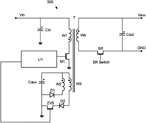
1. A zero-voltage switching (ZVS) flyback converter, comprising:
a transformer having a primary winding, a secondary winding, a first auxiliary winding, and a second auxiliary winding;
an SR switch transistor in series with the secondary winding;
a first diode;
an auxiliary capacitor in series with the first auxiliary winding and the first diode, wherein the first diode is configured to allow a charging current to flow from a positive terminal of the first auxiliary winding into a positive terminal of the auxiliary capacitor and to prevent a current flow into the positive terminal of the first auxiliary winding;
a second diode; and
a ZVS switch transistor in series with the second auxiliary winding and the second diode, wherein the second diode is configured to allow a discharging current to flow from the positive terminal of the auxiliary capacitor through the second auxiliary winding while the ZVS switch transistor is on and to prevent a current flow through the second auxiliary winding while the charging current is conducting.
|