| CPC H02M 3/1584 (2013.01) [G06F 1/3287 (2013.01)] | 20 Claims |

|
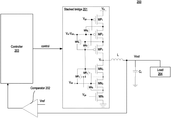
1. An apparatus, comprising:
a high-side section of a stacked bridge, the high-side section comprising a first transistor, second transistor, and third transistor coupled in series, wherein the first transistor is coupled to an input power supply node, and the second transistor is coupled between the first transistor and the third transistor;
a low-side section of the stacked bridge, wherein the low-side section is coupled in series with the high-side bridge at a switching node, the low-side section comprises fourth, fifth, and sixth transistors coupled in series, the fourth transistor is coupled to a ground supply node, and the fifth transistor is coupled between the fourth and sixth transistors; and
first circuitry to pre-charge the switching node before the first transistor is turned on;
wherein the high-side section comprises a seventh transistor coupled in parallel to the first transistor; and
second circuitry to turn on the seventh transistor before turning on the fifth transistor.
|