| CPC H01S 5/0237 (2021.01) [B23K 1/0056 (2013.01); H01S 5/4025 (2013.01); B23K 2101/40 (2018.08)] | 20 Claims |

|
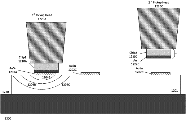
1. A method for performing sequential bonding, said method comprising:
receiving a substrate having a plurality of receiving pads to a stage, wherein a first and second receiving pads of said plurality of receiving pads each comprise a first metal alloy;
attaching a first semiconductor chip to said first receiving pad using a first pickup head, said first semiconductor chip comprising a first metal layer;
raising a temperature of said first semiconductor chip using a first heating unit coupled to said first pickup head according to a first temperature profile to cause intermixing of said first metal layer on said first semiconductor chip and said first metal alloy of said first receiving pad to form a second metal alloy having a higher melting point than said first metal alloy;
attaching a second semiconductor chip to said second receiving pad using a second pickup head, said second semiconductor chip comprising a second metal layer; and
raising a temperature of said second semiconductor chip by a second heating unit coupled to said second pickup head according to a second temperature profile to cause intermixing of said second metal layer on said second semiconductor chip and said first metal alloy of said second receiving pad to form a third metal alloy having a higher melting point than said first metal alloy;
wherein said first predetermined temperature profile comprises temperature set points and time durations and is substantially similar to said second predetermined temperature profile.
|