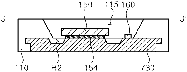
| CPC H01L 33/62 (2013.01) [H01L 33/38 (2013.01); H01L 33/486 (2013.01)] | 21 Claims |

|
1. A light emitting diode package comprising:
a light emitting diode chip including a first electrode pad and a second electrode pad;
a first lead and a second lead spaced apart from each other and electrically connected to the first electrode pad and the second electrode pad of the light emitting diode chip, respectively; and
a housing formed to surround the first lead and the second lead and having a cavity open at a top portion thereof,
wherein the first lead and the second lead have a first lead exposing plane and a second lead exposing plane disposed on a lower surface of the cavity of the housing such that the first lead and the second lead are at least partially exposed and electrically connected to the first electrode pad and the second electrode pad, respectively, and
wherein the first lead exposing plane has a greater width than a width of the light emitting diode chip,
wherein the first lead has a first protrusion protruding outwards from a side surface of the first lead and the second lead has a second protrusion protruding outwards from a side surface of the second lead, and
wherein the first protrusion and the second protrusion extend in directions away from each other,
wherein the first lead and the second lead include a Zener diode mount region and a Zener diode connection region that are portion provided in the cavity to be spaced apart from each other,
wherein a distance from one side of a first groove of the first lead to one side of the first lead exposing plane is greater than a distance from the other side of the first lead exposing plane to one side of the Zener diode mount region.
|