| CPC H01L 33/382 (2013.01) [H01L 27/156 (2013.01); H01L 33/22 (2013.01); H01L 33/405 (2013.01); H01L 33/42 (2013.01); H01L 33/44 (2013.01); H01L 33/62 (2013.01)] | 8 Claims |

|
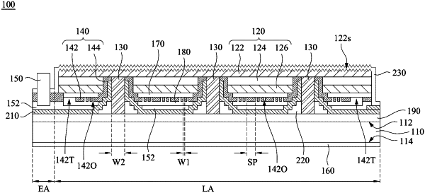
1. A light emitting device, comprises:
a die-bonding substrate having a first surface and a second surface opposite to each other, and the first surface including a light emitting area and an electrode area;
a light emitting semiconductor structure disposed on the light emitting area, and the light emitting semiconductor structure including a first-type semiconductor layer, a light emitting layer and a second-type semiconductor layer from bottom to top;
a plurality of conductive pillars disposed in the light emitting semiconductor structure at intervals, and each of the conductive pillars disposed through the first-type semiconductor layer and the light emitting layer and not disposed through the second-type semiconductor layer, wherein each of the conductive pillars is in direct contact with the second-type semiconductor layer and electrically connected to the die-bonding substrate;
an insulating layer having a first portion and a second portion, the first portion disposed between the first-type semiconductor layer and the die-bonding substrate, and the second portion electrically insulating the first-type semiconductor layer and the light emitting layer from the conductive pillars, wherein the first portion has a trench and a plurality of openings, and the trench is adjacent to an edge of the light emitting semiconductor structure, and a first width of each of the openings is smaller than a second width of each of the conductive pillars;
a first electrode disposed on the electrode area and electrically connected to the first-type semiconductor layer, and the first electrode electrically insulated from each of the conductive pillars;
a second electrode disposed on the second surface and electrically connected to the conductive pillars,
wherein the trench of the first portion of the insulating layer overlaps with the light emitting layer in a vertical direction;
a transparent conductive layer disposed between the first-type semiconductor layer and the first portion, wherein the transparent conductive layer is electrically connected to the first semiconductor layer; and
a first electrode extension portion disposed between the first portion and the die-bonding substrate, the first electrode extension portion electrically connected to the transparent conductive layer through the trench, wherein the first electrode is electrically connected to the first-type semiconductor layer through the first electrode extension portion.
|