| CPC H01L 33/38 (2013.01) [H01L 27/156 (2013.01); H01L 33/486 (2013.01); H01L 33/54 (2013.01); H01L 33/58 (2013.01); H01L 33/62 (2013.01)] | 20 Claims |

|
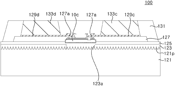
1. A light device, comprising:
a substrate;
two or more light emitting devices disposed on the substrate, each of the two or more light emitting devices comprising a semiconductor layer;
an adhesive layer disposed between a light emitting device and the substrate;
a step adjustment layer covering a region of the light emitting device and comprising a region overlapping the adhesive layer; and
a light block layer disposed on the substrate and configured to provide at least one light path,
wherein the at least one light path includes a concave-convex patterned region disposed between the substrate and the semiconductor layer, and
wherein the at least one light path includes a region comprising a width greater than a width of the light emitting device.
|