US 12,113,146 B2
Optically controlled field effect transistor
Joseph Neil Merrett, Decherd, TN (US)
Assigned to United States of America as represented by the Secretary of the Air Force, Wright-Patterson AFB, OH (US)
Filed by Government of the United States as Represented by the Secretary of the Air Force, Wright-Patterson AFB, OH (US)
Filed on Sep. 9, 2022, as Appl. No. 17/931,067.
Claims priority of provisional application 63/242,168, filed on Sep. 9, 2021.
Prior Publication US 2023/0070932 A1, Mar. 9, 2023
Int. Cl. H01L 31/113 (2006.01)
CPC H01L 31/1136 (2013.01) 12 Claims
OG exemplary drawing
 
1. An optically controlled field effect transistor (FET), comprising:
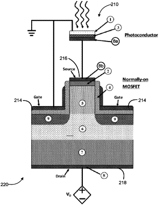
a semiconductor structure configured to form a voltage controlled, normally on, high voltage FET; and
a photoconductive region integrated on the semiconductor structure and configured to reduce a gate-to-source voltage of the FET in response to light incident upon the photoconductive region.