| CPC H01L 31/107 (2013.01) [H01L 31/022466 (2013.01); H01L 31/1804 (2013.01)] | 15 Claims |

|
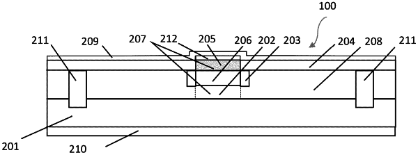
1. A method of manufacturing an avalanche photodetector, the method comprising:
forming a multiplication layer on an entire top surface of a semiconductor wafer,
etching a closed groove on a top surface of the multiplication layer, so that a depth of the closed groove is greater than or equal to a thickness of the multiplication layer, but is smaller than a total thickness of the semiconductor wafer and the multiplication layer combined;
filling the closed groove with highly-doped polycrystalline silicon of the same conductivity type as the multiplication layer;
forming a photodetector inside a region bounded by the closed groove, the photodetector comprising an avalanche amplifier and a photoconverter;
forming at least one avalanche amplifier in the top surface of the multiplication layer in an area bounded by the closed groove, by
(i) etching a circular groove inside a region of the multiplication layer bounded by the closed groove, wherein the circular groove defines the avalanche amplifier, and wherein a depth of the circular groove is less than a thickness of the multiplication layer;
(ii) filling the circular groove with a dielectric material;
(iii) putting a dielectric layer onto surfaces of the multiplication layer and the circular groove;
(iv) filling a window in the dielectric layer with highly doped polycrystalline silicon having an opposite conductivity of the multiplication layer;
(v) placing a contact layer of the avalanche amplifier inside a region bounded by the circular groove, so that the photoconverter is outside the region bounded by the circular groove, such that the photoconverter and the avalanche amplifier are laterally adjacent to each other;
forming a high-resistance layer on the contact layer of the avalanche amplifier;
forming a first electrode made of a transparent material over the high-resistance layer and the dielectric layer;
forming a second electrode on a bottom surface of the semiconductor wafer; and
wherein the high-resistance layer has a resistance of at least 1 megaohm/μm2 at a layer thickness 100 nm.
|