| CPC H01L 31/02027 (2013.01) [G02B 3/06 (2013.01); H01L 27/14605 (2013.01); H01L 27/14621 (2013.01); H01L 27/14627 (2013.01); H01L 27/14629 (2013.01); H01L 27/1463 (2013.01); H01L 27/14643 (2013.01); H01L 27/14649 (2013.01); H01L 31/02327 (2013.01); H01L 31/055 (2013.01); H01L 31/107 (2013.01); H01L 27/1464 (2013.01); H04N 25/63 (2023.01)] | 19 Claims |
|
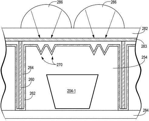
1. A semiconductor device comprising:
a substrate;
a photosensitive area formed in the substrate;
a microlens formed over the photosensitive area; and
a plurality of light scattering structures in the substrate over the photosensitive area, wherein, in a first portion of the substrate, there is a first non-zero number of the light scattering structures per unit area, wherein, in a second portion of the substrate, there is a second non-zero number of the light scattering structures per the unit area, wherein the second non-zero number is greater than the first non-zero number, and wherein the second portion of the substrate forms a ring around the first portion of the substrate.
|