| CPC H01L 31/02027 (2013.01) [H01L 31/022408 (2013.01); H01L 31/0352 (2013.01); H01L 31/107 (2013.01)] | 12 Claims |

|
1. An apparatus, comprising:
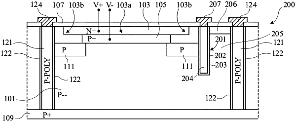
a SPAD-type photodiode comprising:
a depletion area, in which a photogenerated electric charge can be injected to trigger an avalanche of the SPAD-type photodiode, in a first portion of a semiconductor substrate of a first conductivity type;
a gate electrically insulated from the substrate, extending into the substrate from an upper surface of the substrate down to a depth smaller than the thickness of the substrate, and separating the first portion of the substrate from a second portion; and
a first region of the second conductivity type extending from the upper surface of the substrate into the second portion,
wherein the second portion of the substrate does not have a depletion area in which a photogenerated electric charge can be injected to trigger an avalanche of the SPAD-type photodiode.
|