| CPC H01L 29/78693 (2013.01) [H01L 21/02565 (2013.01); H01L 21/02631 (2013.01); H01L 27/1225 (2013.01); H01L 27/127 (2013.01); H01L 29/24 (2013.01); H01L 29/42384 (2013.01); H01L 29/66969 (2013.01); H01L 29/78648 (2013.01); H01L 29/78696 (2013.01); H01L 27/1248 (2013.01); H10K 59/1201 (2023.02); H10K 59/1213 (2023.02); H10K 59/124 (2023.02)] | 20 Claims |

|
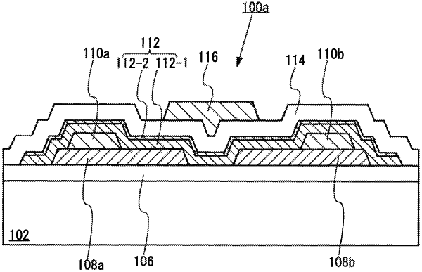
1. A transistor comprising:
an oxide semiconductor layer on a substrate, the oxide semiconductor layer including a first layer and a second layer;
a first gate electrode including a region overlapping the oxide semiconductor layer;
a first insulating layer between the first gate electrode and the oxide semiconductor layer; and
a first oxide conductive layer and a second oxide conductive layer each including a region in contact with the oxide semiconductor layer;
wherein the first layer of the oxide semiconductor layer and the second layer of the oxide semiconductor layer include a region overlapping each other, the first layer of the oxide semiconductor layer is arranged closer to the top surface of the substrate than the second layer of the oxide semiconductor layer,
wherein an energy level at a lower end of the conduction band of the second layer of the oxide semiconductor layer is higher than an energy level at a lower end of the conduction band of the first layer of the oxide semiconductor layer.
|