| CPC H01L 29/66795 (2013.01) [H01L 21/28088 (2013.01); H01L 21/76877 (2013.01); H01L 21/82345 (2013.01); H01L 29/0847 (2013.01); H01L 29/4966 (2013.01); H01L 29/66545 (2013.01); H01L 29/785 (2013.01); H01L 29/7851 (2013.01); H01L 21/76224 (2013.01); H01L 21/823418 (2013.01); H01L 21/823431 (2013.01); H01L 21/823437 (2013.01); H01L 21/823481 (2013.01)] | 20 Claims |
|
1. A device comprising:
a semiconductor region;
a gate dielectric over and contacting the semiconductor region;
a gate electrode over the gate dielectric, wherein the gate electrode comprises:
a metal-containing layer, wherein the metal-containing layer is a work-function layer, and the metal-containing layer comprises:
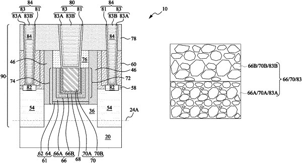
a lower layer having a first average grain size; and
an upper layer over the lower layer, wherein the lower layer and the upper layer comprise a same material, and the upper layer has a second average grain size greater than the first average grain size;
a glue layer over and contacting the work-function layer; and
a metal-filling region over the glue layer; and
source and drain regions on opposing sides of the gate electrode.
|
|
9. A device comprising:
a semiconductor fin;
a gate dielectric on sidewalls and a top surface of the semiconductor fin;
a work-function layer over and contacting the gate dielectric, wherein the work-function layer has a U-shaped cross-sectional view shape, and wherein the work-function layer comprises a first bottom portion and first sidewall portions over and connecting to opposing ends of the first bottom portion, and wherein the work-function layer comprises:
a lower layer having a first average grain size; and
an upper layer over the lower layer, wherein the lower layer and the upper layer comprise a same material, and the upper layer has a second average grain size greater than the first average grain size;
a glue layer over the first bottom portion of the work-function layer, wherein the glue layer comprises a second bottom portion and second sidewall portions over and connecting to the second bottom portion; and
a metal layer having a polycrystalline structure over the second bottom portion of the glue layer.
|
|
16. A device comprising:
a semiconductor fin;
a gate dielectric on sidewalls and a top surface of the semiconductor fin;
a work-function layer over and contacting the gate dielectric, wherein the work-function layer has a polycrystalline structure, and the work-function layer comprises:
a first sub layer of the work-function layer; and
a second sub layer over the first sub layer, wherein the first sub layer and the second sub layer comprise same first elements, and the second sub layer has a different average grain size than the first sub layer; and
a metal layer over the work-function layer, wherein the metal layer comprises:
a third sub layer; and
a fourth sub layer, wherein the third sub layer and the fourth sub layer comprise same second elements, and wherein the fourth sub layer has a different average grain size than the third sub layer.
|