| CPC H01L 29/4236 (2013.01) [H01L 29/401 (2013.01); H01L 29/42364 (2013.01)] | 20 Claims |

|
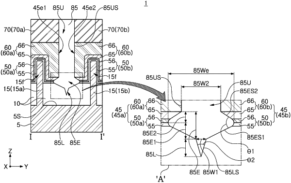
1. A method of manufacturing a semiconductor device comprising:
forming a lower insulating layer on a substrate;
forming an intermediate insulating layer on the lower insulating layer;
forming a conductive structure on the intermediate insulating layer;
forming a preliminary opening penetrating through the conductive structure;
forming an opening by partially etching the intermediate insulating layer and the lower insulating layer, after forming the preliminary opening; and
forming a separation structure in the opening,
wherein the opening divides the conductive structure into a first conductive pattern and a second conductive pattern,
wherein the opening divides the intermediate insulating layer into a first intermediate insulating pattern and a second intermediate insulating pattern,
wherein the separation structure includes:
an intermediate portion between the first intermediate insulating pattern and the second intermediate insulating pattern;
an upper portion upwardly extending from the intermediate portion and between the first conductive pattern and the second conductive pattern; and
a lower portion downwardly extending from the intermediate portion and within the lower insulating layer, and
wherein a maximum width of the intermediate portion is greater than a maximum width of the lower portion.
|