| CPC H01L 29/42316 (2013.01) [H01L 27/098 (2013.01); H01L 29/808 (2013.01); H01L 29/2003 (2013.01)] | 20 Claims |
|
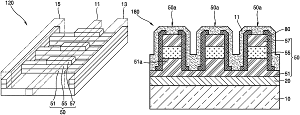
1. A nitride semiconductor device comprising:
a high-resistance material layer including a Group III-V compound semiconductor;
a first channel control layer on the high-resistance material layer and including a Group III-V compound semiconductor of a first conductivity type;
a channel layer on the first channel control layer and including a nitride semiconductor of a second conductivity type opposite to the first conductivity type; and
a gate electrode surrounding the first channel control layer and the channel layer, the gate electrode having a contact of an ohmic contact type with the first channel control layer.
|