| CPC H01L 29/41791 (2013.01) [H01L 27/0924 (2013.01)] | 20 Claims |

|
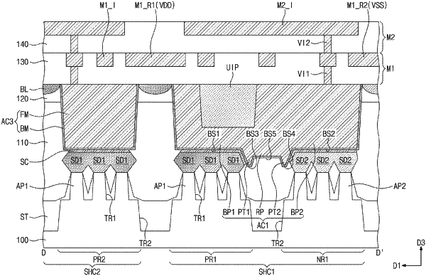
1. A semiconductor device, comprising:
a substrate including a first active region and a second active region adjacent to the first active region in a first direction, the first active region being one of PMOSFET and NMOSFET regions, the second active region being the other one of the PMOSFET and NMOSFET regions;
a device isolation layer on the substrate and defining a first active pattern on the first active region and a second active pattern on the second active region;
a gate electrode extended in the first direction to cross the first and second active patterns;
a first source/drain pattern on the first active pattern and a second source/drain pattern on the second active pattern, wherein each of the first source/drain pattern and the second source/drain pattern is adjacent to a side of the gate electrode;
an interlayer insulating layer on the gate electrode;
a first active contact penetrating the interlayer insulating layer to connect the first source/drain pattern and a second active contact penetrating the interlayer insulating layer to connect the second source/drain pattern; and
a buffer layer provided in an upper region of the interlayer insulating layer and interposed between the first active contact and the second active contact,
wherein upper surfaces of the buffer layer, the first and second active contacts, and the interlayer insulating layer all lie in a same plane, and
wherein the buffer layer includes a material having etch selectivity with respect to the interlayer insulating layer.
|