| CPC H01L 29/1087 (2013.01) [H01L 29/1083 (2013.01); H01L 29/1095 (2013.01); H01L 29/401 (2013.01); H01L 29/41783 (2013.01); H01L 29/47 (2013.01); H01L 29/66484 (2013.01); H01L 29/66696 (2013.01); H01L 29/7816 (2013.01); H01L 29/7831 (2013.01)] | 6 Claims |

|
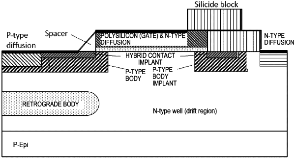
1. A method of fabricating a power transistor structure, comprising the steps of:
(a) providing a substrate of a first dopant polarity;
(b) forming a drift region, of a second dopant polarity, on or within the substrate;
(c) forming a gate structure by oxide growth, polysilicon deposition, and polysilicon etch at least over a portion of the drift region, wherein the gate structure has a source side and a drain side;
(d) implanting a dopant of the first dopant polarity into the drift region on the source side of the gate structure to form a body region, the body region being self-aligned to, and extending under, the gate structure;
(e) implanting a dopant of the second dopant polarity into the self-aligned body region, the implanted dopant defining a hybrid contact implant that has a first depth;
(f) forming a gate sidewall spacer structure such that a first portion of the hybrid contact implant is disposed beneath the gate sidewall spacer structure and a second portion of the hybrid contact implant is exposed adjacent to the gate sidewall spacer structure;
(g) diffusing a dopant of the first dopant polarity into the body region to form a body tap;
(h) applying a photoresist coating to the body region, including the body tap, but leaving the gate structure and drift region entirely or nearly entirely exposed;
(i) diffusing a dopant of the second dopant polarity into the gate structure and into the drift region to form a drain region;
(j) depositing a blanket layer of metal;
(k) annealing the metal of the blanket layer to react with exposed silicon/polysilicon on the body tap, the drain region, the gate structure and the second portion of the hybrid contact implant to form a silicide, wherein the silicide formed on the second portion of the hybrid contact implant has a second depth, and wherein the second depth is greater than the first depth; and
(l) removing unreacted portions of the blanket layer of metal, thereby resulting in metal contacts to the body tap, the drain region, the gate structure, and the hybrid contact implant;
(m) whereby the silicide, the first portion of the hybrid contact implant, and the second portion of the hybrid contact implant together form a hybrid contact, which constitutes a source region, and wherein a channel region is established between the source region and the drift region; and
(n) whereby the resulting hybrid contact defines first, second, and third electrical junctions, wherein the first electrical junction is a Schottky junction formed vertically between the silicide and the substrate, wherein the second electrical junction is an ohmic junction formed laterally between the silicide and the first portion of the hybrid contact implant, and wherein the third electrical junction is a rectifying PN junction between the first portion of the hybrid contact implant and the channel region.
|