| CPC H01L 27/14636 (2013.01) [H01L 27/14609 (2013.01); H01L 27/14623 (2013.01)] | 6 Claims |

|
1. A light receiving element, comprising:
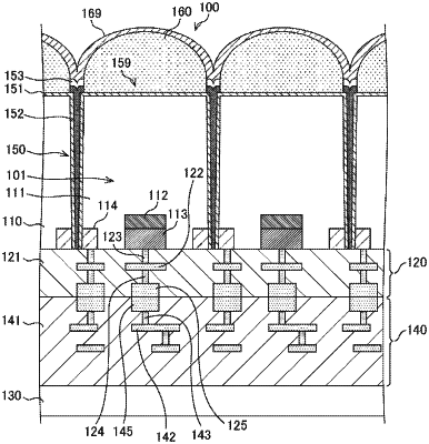
a pixel region in which a plurality of pixels is arranged, the plurality of pixels including a photodiode formed on a semiconductor substrate in which a charge generated by photoelectric conversion of incident light is multiplied with a high reverse bias voltage, an on-chip lens that focuses the incident light on the photodiode, and a wiring region having a wiring layer connected to the photodiode and an insulating layer that insulates the wiring layer; and
an adjacent pixel arranged adjacent to the pixel region and including a photodiode, and a semiconductor region light-blocking wall formed on the semiconductor substrate at a boundary between the pixel region and the adjacent pixel and blocking the incident light.
|