| CPC H01L 27/14636 (2013.01) [G01J 1/44 (2013.01); H01L 31/107 (2013.01); G01J 2001/4466 (2013.01)] | 25 Claims |

|
1. A light detection device, comprising:
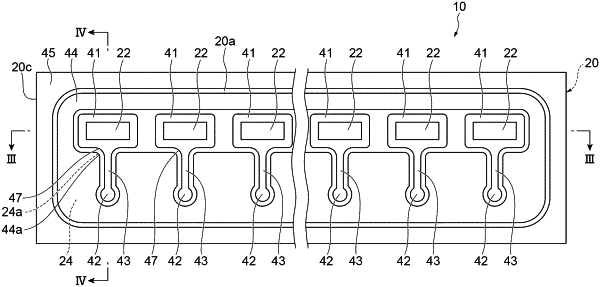
a semiconductor substrate that has first and second main surfaces facing each other and includes a plurality of cells each including at least one avalanche photodiode;
a plurality of pad electrodes arranged on the first main surface so as to be spaced apart from the plurality of cells;
a plurality of wiring portions that are arranged on the first main surface and electrically connect the cells and the pad electrodes, each of the wiring portions electrically connecting the cell and the pad electrode corresponding to each other; and
a plurality of electrode portions each connected to each of the cells,
wherein the avalanche photodiode includes a light absorbing region,
each of the plurality of wiring portions is connected to the electrode portion connected to the cell corresponding thereto,
a connection portion between an edge of the electrode portion and an edge of the wiring portion is curved,
a radius of curvature of the connection portion is equal to or greater than a thickness of the light absorbing region in a thickness direction of the semiconductor substrate,
the semiconductor substrate includes a peripheral carrier absorbing portion configured to absorb carriers located at a periphery of the peripheral carrier absorbing portion, and
the peripheral carrier absorbing portion is provided around each of the pad electrodes and each of the wiring portions when viewed from a direction perpendicular to the first main surface.
|