| CPC H01L 27/1463 (2013.01) [H01L 27/14643 (2013.01)] | 15 Claims |

|
1. An image sensing device comprising:
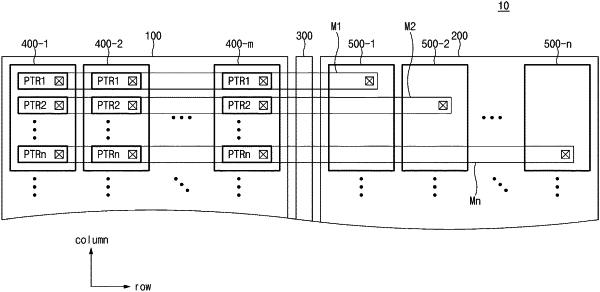
a plurality of unit photosensing pixels structured to convert light into electrical signals, each of the plurality of unit photosensing pixels including a photosensor and a plurality of transistors structured to perform operations associated with the photosensor;
a plurality of protection devices, each of which is coupled to any one of the plurality of transistors; and
an isolation region disposed between a region in which the plurality of protection devices is disposed and a region in which the plurality of unit photosensing pixels is disposed,
wherein each of the plurality of protection devices includes:
a first region doped with a first type of conductive impurities;
a second region doped with a second type of conductive impurities and surrounding the first region; and
a third region doped with the first type of conductive impurities and surrounding the second region,
wherein the first region includes a contact portion and a first well located below the contact portion, and
wherein the contact portion has a higher doping density than the first well, and is coupled to any one of the plurality of transistors, and
wherein the isolation region includes:
a first isolation portion doped with the first type of conductive impurities; and
a second isolation portion doped with the second type of conductive impurities,
wherein the second isolation portion is disposed between a region in which the first isolation portion is disposed and the region in which the plurality of protection devices is disposed, and the second isolation portion is configured to receive a positive voltage, and
wherein the first isolation portion is configured to receive a ground voltage.
|