US 12,113,069 B2
Thermal extraction of single layer transfer integrated circuits
Abhijeet Paul, Poway, CA (US); Richard James Dowling, Temecula, CA (US); Hiroshi Yamada, San Diego, CA (US); Alain Duvallet, San Diego, CA (US); and Ronald Eugene Reedy, San Diego, CA (US)
Assigned to Murata Manufacturing Co., Ltd., Kyoto (JP)
Filed by Murata Manufacturing Co., Ltd., Kyoto (JP)
Filed on Sep. 1, 2022, as Appl. No. 17/901,189.
Application 17/901,189 is a continuation of application No. 17/123,881, filed on Dec. 16, 2020, granted, now 11,437,404.
Application 17/123,881 is a continuation of application No. PCT/US2019/041898, filed on Jul. 15, 2019.
Application PCT/US2019/041898 is a continuation of application No. 16/040,295, filed on Jul. 19, 2018, granted, now 10,658,386, issued on May 19, 2020.
Prior Publication US 2023/0072271 A1, Mar. 9, 2023
Int. Cl. H01L 21/00 (2006.01); H01L 21/48 (2006.01); H01L 21/8234 (2006.01); H01L 21/84 (2006.01); H01L 23/373 (2006.01); H01L 27/092 (2006.01); H01L 27/12 (2006.01)
CPC H01L 27/1203 (2013.01) [H01L 21/4882 (2013.01); H01L 21/823481 (2013.01); H01L 21/84 (2013.01); H01L 23/3735 (2013.01); H01L 27/092 (2013.01)] 4 Claims
OG exemplary drawing
 
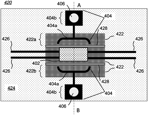
1. A method of making a thermal conduction structure for an integrated circuit transistor device, including:
(a) fabricating at least one dummy gate electrically isolated from the transistor device by a gate oxide and in thermal contact with the transistor device;
(b) fabricating at least one thermal path electrically isolated from the transistor device and in thermal contact with at least one dummy gate, the at least one thermal path configured to convey heat from the transistor device to a heat sink.