| CPC H01L 27/0924 (2013.01) [H01L 21/823821 (2013.01); H01L 29/0673 (2013.01); H01L 29/42392 (2013.01); H01L 29/66545 (2013.01); H01L 29/775 (2013.01)] | 22 Claims |

|
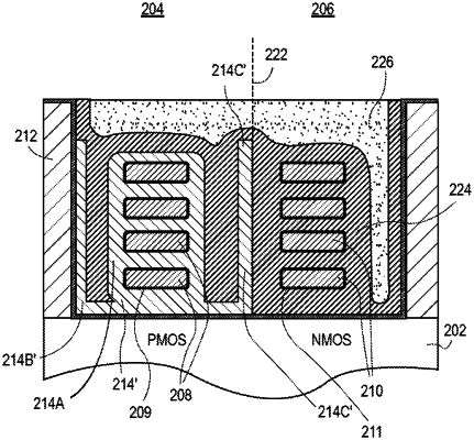
1. An integrated circuit structure, comprising:
a first vertical arrangement of horizontal nanowires;
a second vertical arrangement of horizontal nanowires;
a first gate stack over the first vertical arrangement of horizontal nanowires, the first gate stack having a P-type conductive layer with a first portion surrounding the nanowires of the first vertical arrangement of horizontal nanowires and a second portion extending laterally beside and spaced apart from the first portion, wherein the second portion of the P-type conductive layer is laterally between the first vertical arrangement of horizontal nanowires and the second vertical arrangement of horizontal nanowires, the second portion of the P-type conductive layer having a first sidewall and a second sidewall laterally opposite to the first sidewall, wherein the first sidewall and the second sidewall are vertical sidewalls of a same continuous portion of the P-type conductive layer, and wherein the second portion of the P-type conductive layer has an uppermost surface above an uppermost surface of one or more of the nanowires of the first vertical arrangement of horizontal nanowires or the second vertical arrangement of horizontal nanowires; and
a second gate stack over the second vertical arrangement of horizontal nanowires, the second gate stack having an N-type conductive layer with a first portion surrounding the nanowires of the second vertical arrangement of horizontal nanowires and a second portion adjacent to and in contact with the first sidewall and the second sidewall of the second portion of the P-type conductive layer.
|