| CPC H01L 27/0886 (2013.01) [H01L 21/823418 (2013.01); H01L 21/823431 (2013.01); H01L 29/0847 (2013.01); H01L 29/66795 (2013.01); H01L 29/7851 (2013.01)] | 19 Claims |

|
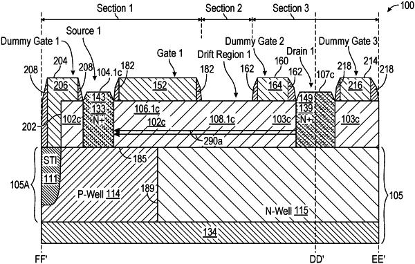
1. A fin-based field effect transistor (finFET) device, comprising:
a fin structure comprising a first portion, a second portion, a third portion, a fourth portion and a fifth portion;
a first gate structure disposed over at least part of the first portion and a second gate structure disposed over at least part of the fifth portion;
a first source/drain region disposed in the first portion;
a second drain/source region disposed in the third portion; and
a third source/drain region disposed in the fifth portion;
wherein:
each of the first, second and third portions comprises one or more fin portions; and
a total number of fin portions in the second portion is fewer than a total number of fin portions in the first portion and a total number of fin portions in the fourth portion is fewer than a total number of fin portions in the fifth portion.
|