| CPC H01L 27/0605 (2013.01) [H01L 29/2003 (2013.01); H01L 29/205 (2013.01); H01L 29/7786 (2013.01)] | 19 Claims |

|
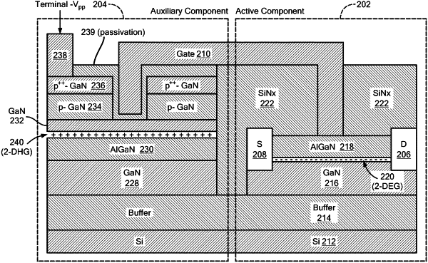
1. A semiconductor device comprising:
an active component comprising:
a first narrow-bandgap material layer; and
a first wide-bandgap material layer disposed over the first narrow-bandgap material layer and having first, second and third electrical connections with an interface between the first narrow-bandgap material layer and the first wide-bandgap material layer corresponding to a negatively charged carrier channel with a gate terminal disposed on the first wide-bandgap material layer; and
an auxiliary component comprising:
a second narrow-bandgap material layer;
a second wide-bandgap material layer disposed over the second wide-bandgap material layer with an interface between second narrow-bandgap material layer and second wide-bandgap material layer corresponding to a negatively charged carrier channel;
a third narrow-bandgap material layer disposed over the second wide-bandgap material layer with an interface between the third narrow-bandgap material layer and the second wide-bandgap material layer corresponding to a positively charged carrier channel with a gate terminal disposed on the third narrow-bandgap material layer; and
a fourth narrow-bandgap material layer disposed over the third narrow-bandgap material layer; and
a bias electrode disposed over fourth narrow-bandgap material layer; and
means for electrically connecting the gate terminal of the auxiliary component to the gate terminal of the active component.
|