| CPC H01L 27/0255 (2013.01) [H01L 27/0292 (2013.01); H01L 27/0288 (2013.01); H01L 27/0296 (2013.01)] | 17 Claims |

|
1. A display device comprising:
a substrate including a display area containing a plurality of pixels and a non-display area surrounding the display area;
a semiconductor layer including a transistor having a source area, a channel area, and a drain area, the transistor disposed in the non-display area of the substrate;
a gate electrode of the transistor overlapping the channel area of the semiconductor layer;
a gate insulating layer disposed between the gate electrode and the channel area of the semiconductor layer;
a source electrode electrically connected to the source area of the semiconductor layer; and
a drain electrode electrically connected to the drain area of the semiconductor layer, wherein
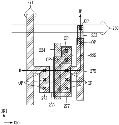
both lateral sides of the gate electrode facing each other overlap the drain electrode in a direction perpendicular to the substrate,
the gate electrode includes an expansion not overlapping the semiconductor layer in the direction perpendicular to the substrate,
the expansion of the gate electrode overlaps the drain electrode in the direction perpendicular to the substrate,
an interlayer insulating layer is disposed between the expansion of the gate electrode and the drain electrode,
the interlayer insulating layer includes an opening,
the expansion of the gate electrode is electrically connected to the drain electrode in the opening, and
the gate electrode comprises:
a portion that overlaps the drain electrode in the direction perpendicular to the substrate and another portion that does not overlap the drain electrode in the direction perpendicular to the substrate, the another portion having a wider width than the portion that overlaps the drain electrode.
|