| CPC H01L 25/50 (2013.01) [H01L 21/304 (2013.01); H01L 21/306 (2013.01); H01L 21/3081 (2013.01); H01L 21/561 (2013.01); H01L 21/683 (2013.01); H01L 23/3121 (2013.01); H01L 23/3135 (2013.01); H01L 25/0657 (2013.01); H01L 2225/06513 (2013.01); H01L 2225/06541 (2013.01); H01L 2924/1304 (2013.01); H01L 2924/1434 (2013.01); H01L 2924/1461 (2013.01); H01L 2924/351 (2013.01); H01L 2924/3511 (2013.01)] | 53 Claims |

|
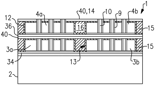
1. A bonded structure comprising:
a carrier;
a first die layer comprising:
a first surface and a second surface opposite the first surface, the first surface directly bonded to the carrier without an intervening adhesive, the second surface comprising a first non-conductive region and a first conductive region;
a first integrated device die; and
a first protective material comprising a first layer disposed along a sidewall of the first integrated device die and a second layer on the first layer, each of the first and second layers comprising a silicon-containing inorganic dielectric material; and
a second die layer comprising:
a third surface comprising a second non-conductive region directly bonded to the first non-conductive region and a second conductive region directly bonded to the first conductive region; and
a second integrated device die.
|