| CPC H01L 25/18 (2013.01) [H01L 24/08 (2013.01); H01L 25/0657 (2013.01); H01L 2224/08145 (2013.01); H01L 2924/1431 (2013.01); H01L 2924/1436 (2013.01); H01L 2924/14511 (2013.01)] | 19 Claims |

|
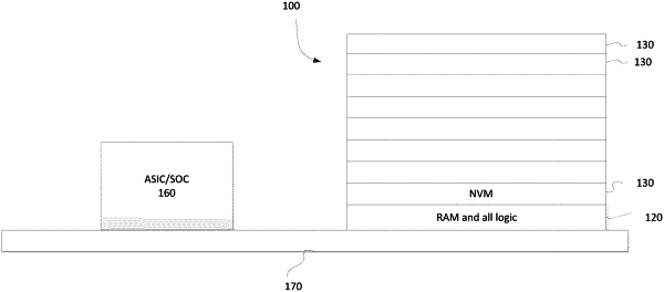
1. A stacked memory device, comprising:
a first layer comprising random access memory (RAM); and
a plurality of second layers vertically stacked above the first layer, each of the plurality of second layers comprising multiple blocks of nonvolatile memory (NVM),
wherein the first layer is directly bonded to an adjacent one of the second layers without an intervening material layer therebetween; and
wherein interconnects of the first layer are directly bonded to interconnects of the adjacent one of the second layers to form a plurality of parallel input/output (I/O) paths between the RAM and the NVM, wherein the parallel I/O paths are at least 1 k bits wide.
|